


In automotive applications, GaN DC-DC converter suffers severe reliability issues. Figure 1 shows a typical DC-DC converter, which employs GaN power switches for high efficient and high fSW operation to increase transient response, and reduce solution size, thermal generation and cost. However, two main challenges need to be resolved before its use in automotive.
Firstly, in a buck conversion as shown in Figure 1, due to the absent of body diode in the bottom GaN transistor ML, the switching node voltage VSW could go negative during VSW falling and rising edge intervals. For example, during the VSW falling edge interval, ML becomes reversely conducted to freewheel the inductor current, and VSW goes to −3V. With a constant gate driver power supply voltage VDRV, destructive overcharge happens at the bootstrap capacitor CBST. With a 5V VDRV, VSW can fall to −3V forcing CBST and thus the BST rail to be overcharged, which exceeds the VGS maximum rating of GaN FET and causes gate breakdown and destructive damage to the high side GaN FET power switch.

Figure 1 A typical GaN based DC-DC converter in automotive applications
Power Efficiency and Thermal Challenges
With the ever-increasing power level and power dissipation, the GaN DC-DC converters suffer severe thermal problems. Figure 2 shows the thermal distribution map of a typical GaN based DC-DC converter which converts a voltage of 48V to 12V with a buck topology at 300KHz switching frequency. However, due to the high-power level up to 360W and high-power dissipation, the peak temperature at the GaN FETs is nearly 100. Moreover, the miniaturization of GaN transistors and the WLCSP package make the thermal dissipation more challenging, thus a more efficient power conversion is required which reduces the power loss and thermal generation.
The power loss of the DC-DC converter mainly consists three categories: the conduction loss, the switching loss and the gate charge loss. To reduce the conduction loss in GaN power switches, the gate driver voltage needs to be maximized to effective reduce the on-resistance. Typically, the drive rail voltages VDRV are generated either stepping down from the high voltage bus with a linear regulator, or directly from the low output voltage with a controlled power switch. However, both approaches degrade the system efficiency. With a much less gate in GaN switches, a much lower gate charge loss and switching loss in each switching period are achieved. However, as the switching frequency is pushed high to reduce system solution size, the switching loss becomes dominant especially at light load condition.
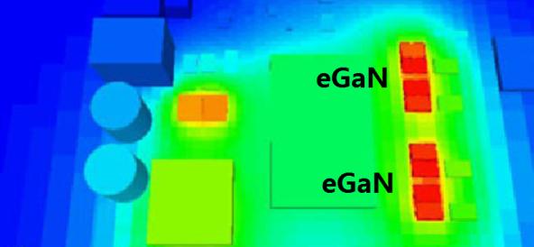
Figure 2 Thermal distribution map of a typical GaN based DC-DC converter
EMI Challenges
The electromagnetic interference (EMI) noise becomes a major challenge that must be overcome before using GaN in automotive applications . Firstly, the fixed gate driving technique in GaN converters incurs high di/dt and dv/dt transitions which cause high frequency EMI noise that spreads through input bus. In a GaN based DC-DC converter as shown in Figure 3, the fixed gate driving incurs high speed transitions of switching node voltage (VSW) and drain current of high side GaN FET MH. This could create unwanted noise or even a malfunction in the safety-related systems. A bulky input filter is conventionally employed to reduce EMI noise at VIN bus, but it dramatically increases system volume and cost.
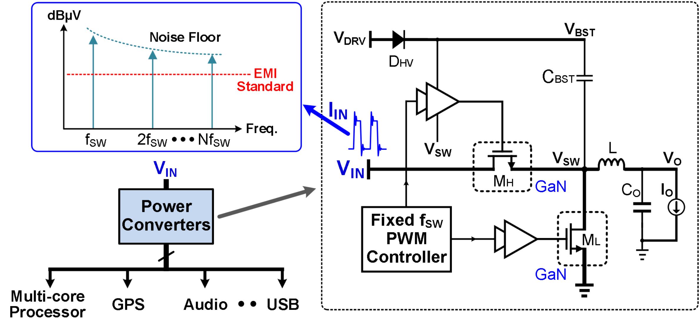
Figure 3 EMI challenges of fixed frequency GaN based DC-DC converter.
High Frequency Switching Challenges
In order to operate at high switching frequencies up to tens of megahertz, conventional GaN gate drivers have some problems. Figure 4 depicts noise and transitions on the GND signal due to parasitics at the chip, package, or PCB level. At the same time, the dv/dt of the switching node VSW of GaN can usually reach more than 100V/ns. In conventional GaN gate drivers, the traditional level shifter has weak common-mode rejection and asymmetric gate driving propagation delay, which will cause the error of the driving signal and lead to the safety issue of the system. Relying on the core technologies, PRIMECHIP can solve the GaN drive and control issues while realizing high performance, high stability and high reliability of the GaN DC-DC power systems. (Copyright at PRIMECHIP)
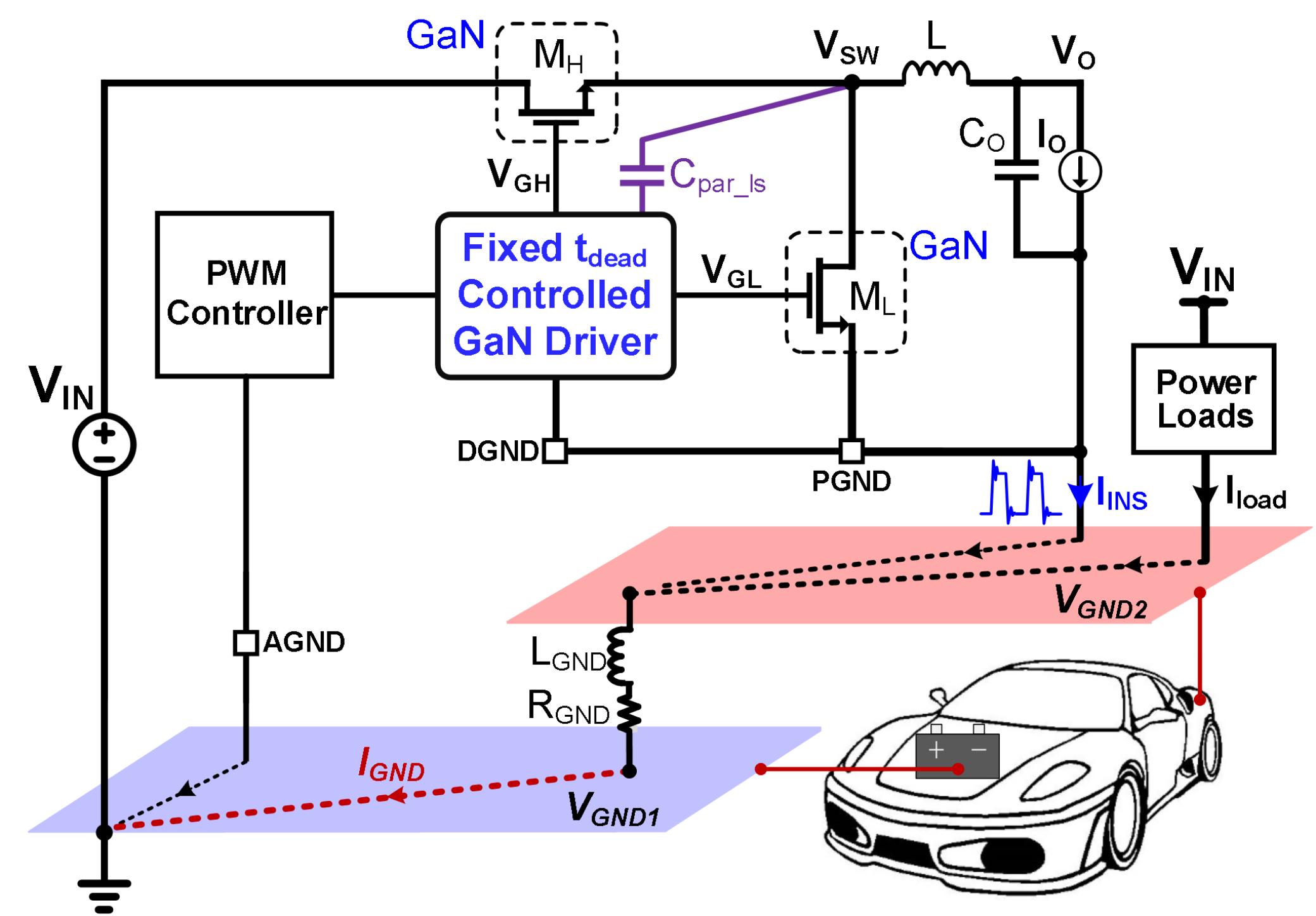
Figure 4 High frequency switching challenges in GaN based DC-DC converter.