


Gallium nitride is a compound semiconductor material composed of nitrogen and gallium. Due to a wide band gap votlage greater than 2.2eV, Gallium Nitride (GaN), Silicon Carbide (SiC), Aluminum Nitride (AlN), Gallium Oxide (Ga2O3), etc., are collectively referred as wide band gap semiconductor materials, also known as the third generation semiconductors.
Compared to silicon (Si) and silicon carbide (SiC) couterparts, Gallium Nitride shows a higher bandgap voltage and higher critical electrical field, resulting in a high breakdown voltage (or equivalent breakdown voltage and on-resistance but with a much smaller size). Figure 1 shows the on-resistance and breakdown voltage comparison of the state-of-art Si, SiC, and GaN power devices. The specific on-resistance RON, SP is defined as the on-resistance RON offered by a given die size A, which is given by

where VBV is the breakdown voltage, μn is the mobility of electrons, εr is the relative permittivity, ε0 is the vacuum permittivity, and Ecrit is the critical electrical field of the avalanche breakdown.

Figure 1. On-resistance vs. breakdown voltage comparison for Si, SiC, and GaN devices.
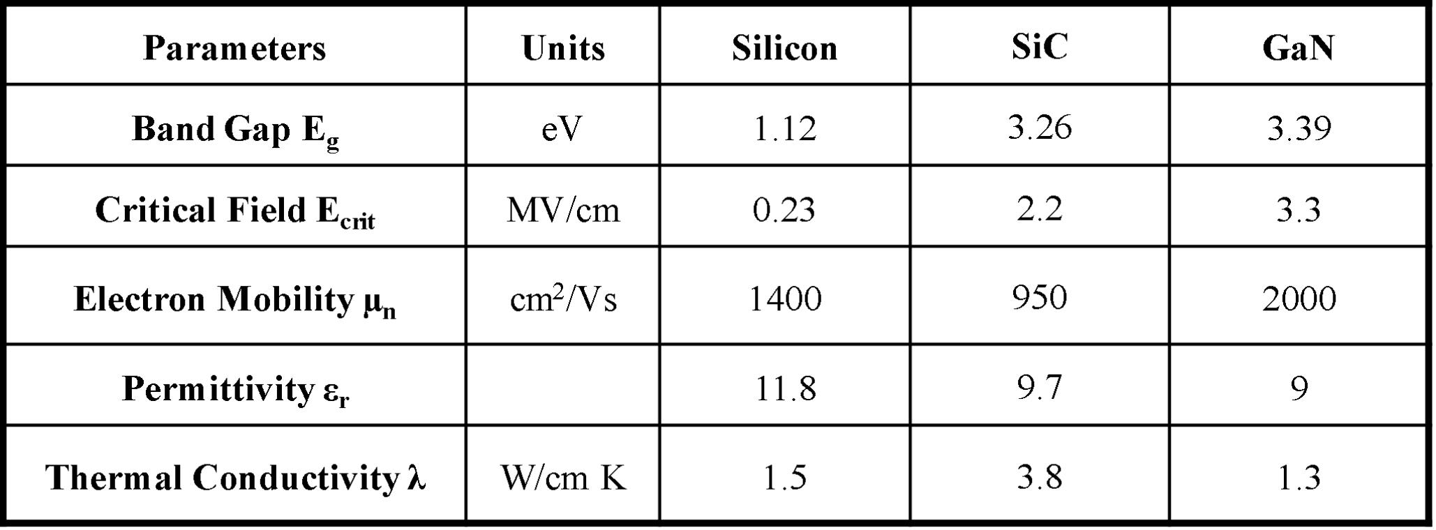
Table 1. Material Properties of Silicon, SiC and GaN.
Substitute the equation above with the properties of silicon, SiC and GaN, as shown in Table 1, the theoretical limit is calculated and depicted as shown in Figure 1. The theoretical limit of GaN is much higher than Si and SiC which means GaN demonstrates a much higher breakdown voltage under a similar RON, SP, or equivalently a much smaller size with a same breakdown voltage. Furthermore, GaN transistor shows a high electron mobility in Table 1, which significantly reduces the on-resistance and conduction loss in power converters. Moreover, with a smaller size, the parasitic capacitance of GaN transistor dramatically decreases, which makes it highly suited for high frequency switching mode power converter applications.
DC-DC converters have gained more popularity due to the high efficiency, compared to linear regulator solutions. To meet the demands for high power density, low solution size and fast transient response, pushing the switching frequency (fSW) to high becomes inevitable. However, the power efficiency degrades significantly as the switching loss increases with the conventional silicon FET. As discussed previously, GaN FETs have demonstrated superior figure-of-merits as power switches in alleviating these challenges. Figure 2 shows the turn-on behavior of GaN power switch in comparison with silicon power switch. Due to smaller parasitic capacitance (Cgs, Cgd and Cds), smaller input and output charges (Qg, Qoss) and near-zero reverse recovery (absence of body diode), GaN FET shows much shorter turn-on transition periods. As shown in Figure 2, the turn-on switching loss is a simultaneous exposure of the switch to a significant voltage and current experienced during turn-on, which is depicted as an area of Ploss. Thus, with a much shorter transition period from t1 to t3 (including di/dt, dv/dt transition periods), GaN FETs bring a significant reduction in switching loss, thus enable highly efficient power conversion at high fSW to reduce the system size and cost.
The proprietary gallium nitride power products and solutions created by PRIMECHIP are greatly reducing the conduction losses and switching losses, significantly improving the power conversion efficiency of the system to meet the urgent requirements of carbon neutrality, thereby meeting the needs of data centers, electric vehicles and high-end consumer electronics. (Copyright at PRIMECHIP)
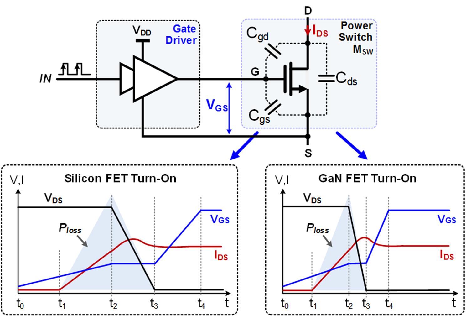
Figure 2. Turn-on behavior of silicon FET and GaN FET power switches.