1-1

What is GaN FET Power Transistor?

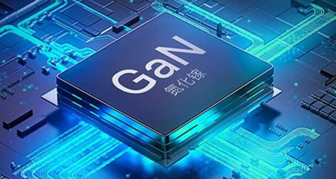
Gallium nitride is a compound semiconductor material composed of nitrogen and gallium. Due to a wide band gap votlage greater than 2.2eV, Gallium Nitride (GaN), Silicon Carbide (SiC), Aluminum Nitride (AlN), Gallium Oxide (Ga2O3), etc., are collectively referred as wide band gap semiconductor materials, also known as the third generation semiconductors.

Compared to silicon (Si) and silicon carbide (SiC) couterparts, Gallium Nitride shows a higher bandgap voltage and higher critical electrical field, resulting in a high breakdown voltage (or equivalent breakdown voltage and on-resistance but with a much smaller size). Figure 1 shows the on-resistance and breakdown voltage comparison of the state-of-art Si, SiC, and GaN power devices. The specific on-resistance RON, SP is defined as the on-resistance RON offered by a given die size A, which is given by

where VBV is the breakdown voltage, μn is the mobility of electrons, εr is the relative permittivity, ε0 is the vacuum permittivity, and Ecrit is the critical electrical field of the avalanche breakdown.

Figure 1. On-resistance vs. breakdown voltage comparison for Si, SiC, and GaN devices.

Table 1. Material Properties of Silicon, SiC and GaN.


Substitute the equation above with the properties of silicon, SiC and GaN, as shown in Table 1, the theoretical limit is calculated and depicted as shown in Figure 1. The theoretical limit of GaN is much higher than Si and SiC which means GaN demonstrates a much higher breakdown voltage under a similar RON, SP, or equivalently a much smaller size with a same breakdown voltage. Furthermore, GaN transistor shows a high electron mobility in Table 1, which significantly reduces the on-resistance and conduction loss in power converters. Moreover, with a smaller size, the parasitic capacitance of GaN transistor dramatically decreases, which makes it highly suited for high frequency switching mode power converter applications.

DC-DC converters have gained more popularity due to the high efficiency, compared to linear regulator solutions. To meet the demands for high power density, low solution size and fast transient response, pushing the switching frequency (fSW) to high becomes inevitable. However, the power efficiency degrades significantly as the switching loss increases with the conventional silicon FET. As discussed previously, GaN FETs have demonstrated superior figure-of-merits as power switches in alleviating these challenges. Figure 2 shows the turn-on behavior of GaN power switch in comparison with silicon power switch. Due to smaller parasitic capacitance (Cgs, Cgd and Cds), smaller input and output charges (Qg, Qoss) and near-zero reverse recovery (absence of body diode), GaN FET shows much shorter turn-on transition periods. As shown in Figure 2, the turn-on switching loss is a simultaneous exposure of the switch to a significant voltage and current experienced during turn-on, which is depicted as an area of Ploss. Thus, with a much shorter transition period from t1 to t3 (including di/dt, dv/dt transition periods), GaN FETs bring a significant reduction in switching loss, thus enable highly efficient power conversion at high fSW to reduce the system size and cost.

The proprietary gallium nitride power products and solutions created by PRIMECHIP are greatly reducing the conduction losses and switching losses, significantly improving the power conversion efficiency of the system to meet the urgent requirements of carbon neutrality, thereby meeting the needs of data centers, electric vehicles and high-end consumer electronics. (Copyright at PRIMECHIP)

Figure 2. Turn-on behavior of silicon FET and GaN FET power switches.


4-5

Challenges of GaN DC-DC Conversion

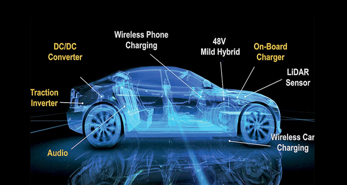
Stimulated by the fast-increasing applications and the newly emerging GaN technology, the switching power converters are developed to the next-generation with fast transient response, small solution size, high integration and high-power density, making it suited for datacenter and automotive applications. With a much smaller gate capacitance and high channel conductivity in GaN devices, a high conversion efficiency can be achieved, reducing the solution size and cost. However, there are still some challenges of reliability, efficiency, EMI and high frequency switching in GaN DC-DC conversion before its wide application in automotive. To have a better understanding on these critical issues, these four types of challenges are briefly discussed in the following sessions.
Reliability Challenges
In automotive applications, GaN DC-DC converter suffers severe reliability issues. Figure 1 shows a typical DC-DC converter, which employs GaN power switches for high efficient and high fSW operation to increase transient response, and reduce solution size, thermal generation and cost. However, two main challenges need to be resolved before its use in automotive.
Firstly, in a buck conversion as shown in Figure 1, due to the absent of body diode in the bottom GaN transistor ML, the switching node voltage VSW could go negative during VSW falling and rising edge intervals. For example, during the VSW falling edge interval, ML becomes reversely conducted to freewheel the inductor current, and VSW goes to −3V. With a constant gate driver power supply voltage VDRV, destructive overcharge happens at the bootstrap capacitor CBST. With a 5V VDRV, VSW can fall to −3V forcing CBST and thus the BST rail to be overcharged, which exceeds the VGS maximum rating of GaN FET and causes gate breakdown and destructive damage to the high side GaN FET power switch.
Secondly, fixed dead time (tdead) control is used to prevent disastrous shoot-through current in GaN power switches. However, since the falling edge slope of VSW is inversely proportional to IO, fixed tdead control is problematic. The charge at CSW is discharged quickly with a high peak IO, resulting in a high falling slope of VSW. With a fixed tdead, VSW drops down and reaches 0V before the tdead expires, and ML becomes reversely conducted to freewheel inductor current which leads to a high reverse conduction loss. On the contrary, in small IO, the charge at CSW is discharged with a low level of IL, leading to a slow falling slope. And a fixed tdead causes an excessive switching charge loss. And VSW falling time is proportional on VIN level, fixed tdead control causes high power loss. Thus, fixed tdead causes either a reverse conduction loss or a high switching charge loss. Moreover, at a high fSW up to tens of MHz, the power loss due to fixed tdead control becomes significantly high.


Figure 1 A typical GaN based DC-DC converter in automotive applications


Power Efficiency and Thermal Challenges
With the ever-increasing power level and power dissipation, the GaN DC-DC converters suffer severe thermal problems. Figure 2 shows the thermal distribution map of a typical GaN based DC-DC converter which converts a voltage of 48V to 12V with a buck topology at 300KHz switching frequency. However, due to the high-power level up to 360W and high-power dissipation, the peak temperature at the GaN FETs is nearly 100. Moreover, the miniaturization of GaN transistors and the WLCSP package make the thermal dissipation more challenging, thus a more efficient power conversion is required which reduces the power loss and thermal generation.

The power loss of the DC-DC converter mainly consists three categories: the conduction loss, the switching loss and the gate charge loss. To reduce the conduction loss in GaN power switches, the gate driver voltage needs to be maximized to effective reduce the on-resistance. Typically, the drive rail voltages VDRV are generated either stepping down from the high voltage bus with a linear regulator, or directly from the low output voltage with a controlled power switch. However, both approaches degrade the system efficiency. With a much less gate in GaN switches, a much lower gate charge loss and switching loss in each switching period are achieved. However, as the switching frequency is pushed high to reduce system solution size, the switching loss becomes dominant especially at light load condition.


Figure 2 Thermal distribution map of a typical GaN based DC-DC converter


EMI Challenges
The electromagnetic interference (EMI) noise becomes a major challenge that must be overcome before using GaN in automotive applications . Firstly, the fixed gate driving technique in GaN converters incurs high di/dt and dv/dt transitions which cause high frequency EMI noise that spreads through input bus. In a GaN based DC-DC converter as shown in Figure 3, the fixed gate driving incurs high speed transitions of switching node voltage (VSW) and drain current of high side GaN FET MH. This could create unwanted noise or even a malfunction in the safety-related systems. A bulky input filter is conventionally employed to reduce EMI noise at VIN bus, but it dramatically increases system volume and cost.


Figure 3 EMI challenges of fixed frequency GaN based DC-DC converter.


High Frequency Switching Challenges
In order to operate at high switching frequencies up to tens of megahertz, conventional GaN gate drivers have some problems. Figure 4 depicts noise and transitions on the GND signal due to parasitics at the chip, package, or PCB level. At the same time, the dv/dt of the switching node VSW of GaN can usually reach more than 100V/ns. In conventional GaN gate drivers, the traditional level shifter has weak common-mode rejection and asymmetric gate driving propagation delay, which will cause the error of the driving signal and lead to the safety issue of the system. Relying on the core technologies, PRIMECHIP can solve the GaN drive and control issues while realizing high performance, high stability and high reliability of the GaN DC-DC power systems. (Copyright at PRIMECHIP)

Figure 4 High frequency switching challenges in GaN based DC-DC converter.